Mastering STM32 MCU Pins: A Comprehensive Guide for Embedded Developers
Introduction
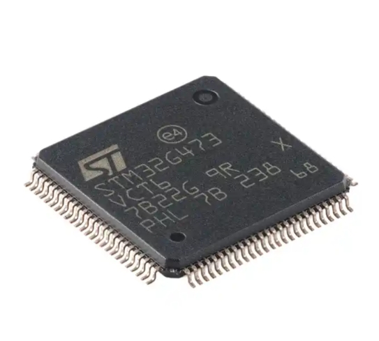
In the realm of embedded systems and microcontroller development, few platforms command as much respect and widespread adoption as the STM32 family by STMicroelectronics. At the heart of every STM32-based project lies a critical, yet sometimes overlooked, aspect: the configuration and management of its General-Purpose Input/Output (GPIO) pins. These tiny metallic connections are the vital bridge between the intelligent silicon brain of the Microcontroller Unit (MCU) and the external world of sensors, actuators, displays, and communication modules. A deep and practical understanding of STM32 MCU pins is not merely a technical detail; it is a fundamental skill that separates novice programmers from proficient embedded engineers. This guide delves into the architecture, functionality, and strategic use of these pins, empowering you to unlock the full potential of your STM32 projects. For developers seeking to streamline their component selection process for such projects, platforms like ICGOODFIND can be invaluable resources for sourcing reliable electronic components.

Part 1: Understanding STM32 Pin Architecture and Alternate Functions
STM32 MCUs are built around ARM Cortex-M cores, but their true versatility is exposed through their pinout. Unlike simpler microcontrollers, most pins on an STM32 are multifunctional, a feature central to their flexibility.
Pin Structure and GPIO Registers: Each GPIO port (e.g., GPIOA, GPIOB, GPIOC) is controlled by a set of memory-mapped registers. Key registers include: * MODER (Mode Register): This is the most fundamental control. It configures each pin as an input, output, alternate function, or analog mode. Misconfiguring this register is a common source of issues. * OTYPER (Output Type Register): Determines if an output pin operates as a push-pull or open-drain. Push-pull is standard for direct driving, while open-drain is essential for I2C communication and wired-AND configurations. * OSPEEDR (Output Speed Register): Controls the slew rate—how fast the pin can switch between logical high and low. Higher speed settings are crucial for high-frequency signals like SPI or USB but can increase electromagnetic interference (EMI). * PUPDR (Pull-up/Pull-down Register): Enables internal resistors to pull the pin to a defined state (VDD or GND) when it is not being actively driven, preventing it from floating and picking up noise.
The Power of Alternate Functions (AF): This is where STM32 pins shine. A single physical pin can serve multiple purposes. For instance, Pin PA2 might be: * A simple GPIO output (LED control). * USART2_TX for serial communication (Alternate Function 7). * TIM2_CH3 for PWM output (Alternate Function 1). * An ADC input in analog mode.
The specific alternate function mapping is defined in the MCU’s datasheet in the “Pinouts and pin description” section and is managed by the Alternate Function Register (AFR). Using HAL libraries or CubeMX, this configuration is often abstracted, but understanding the underlying mechanism is key for debugging and advanced optimization.
Part 2: Practical Configuration and Common Interfaces
Moving from theory to practice involves correctly initializing pins for specific tasks. Modern development typically uses STM32CubeIDE and its graphical tool, STM32CubeMX, which generates initialization code.
Configuration Workflow: 1. Clock Enable: Before accessing any peripheral or GPIO port, its clock must be enabled via the RCC (Reset and Clock Control) registers. CubeMX does this automatically. 2. Mode Selection: Choose the correct mode in MODER. For a UART TX pin, it must be set to Alternate Function mode. 3. Alternate Function Selection: Select the precise AF number (e.g., AF07 for USART2) in the AFR register. 4. Output Type & Speed: For an output like TX, use Push-Pull with a medium-to-high speed depending on the baud rate. 5. Pull-up/down: For an I2C data line (SDA), you would typically configure it as open-drain and enable the internal pull-up resistor.
Key Communication Interfaces and Their Pin Demands: * UART/USART: Requires minimum two pins: TX (output) and RX (input). Configuration is relatively straightforward but ensuring the correct AF is crucial. * SPI: A more complex interface requiring four pins: SCK (clock), MOSI (Master Out Slave In), MISO (Master In Slave Out), and NSS (Chip Select). All operate at high speed; thus, pin output speed must be configured appropriately. * I2C: Uses two bidirectional open-drain lines: SDA (Data) and SCL (Clock). The open-drain configuration and external or internal pull-up resistors are mandatory for proper operation. * ADC (Analog-to-Digital Converter): Pins must be placed in Analog Mode (MODER = 11). In this mode, digital input Schmitt triggers are disabled, and the pin is connected directly to the ADC’s sampling circuit.
Part 3: Advanced Considerations and Best Practices
Efficiently managing dozens of multifunctional pins requires foresight and strategy.
Pin Planning and Conflict Resolution: During schematic design, carefully consult the MCU’s datasheet to avoid pin function conflicts. A pin used for ADC input cannot simultaneously serve as a PWM output. Tools like CubeMX provide a visual conflict checker, which is indispensable for complex projects. Planning involves considering not just primary functions but also future debugging needs—reserving a pin for an LED or UART debug output can save immense time later.
Power, Layout, and ESD Protection: * Power Pins: Never neglect power supply pins (VDD/VSS pairs). Each pair should be decoupled with a 100nF ceramic capacitor placed as close as possible to the MCU. Some high-performance STM32s have separate analog power pins (VDDA/VSSA) that must be properly supplied for accurate ADC/DAC operation. * Unused Pins: As a best practice, configure unused pins as analog inputs or outputs with pull-downs to minimize power consumption and noise susceptibility. * Robustness: In industrial or noisy environments, external protection such as series resistors for current limiting or TVS diodes for ESD protection may be necessary on GPIOs connected to connectors.
Debugging Pin-Related Issues: Common problems include: * Pin not responding: Check clock enable (RCC) and mode register (MODER). * Incorrect signal levels: Verify OTYPER (push-pull vs. open-drain) and PUPDR settings. * Signal integrity issues (ringing, noise): Re-evaluate OSPEEDR settings—sometimes reducing speed improves signal quality. Ensure proper PCB layout with short traces.
Leveraging community resources and component databases like ICGOODFIND can help quickly identify alternative parts or find application notes related to specific pin configurations when tackling unique challenges.
Conclusion
The humble pin is the gateway through which an STM32 MCU interacts with its application. Mastering its architecture—from basic GPIO modes to complex alternate function mappings—is foundational to successful embedded design. This involves not just knowing which register to set but understanding the implications of those settings on system performance, power consumption, and reliability. By methodically planning pin assignments, adhering to configuration best practices for different communication protocols, and considering advanced aspects like power integrity and noise immunity, developers can build robust and efficient systems. The flexibility of STM32 pins is one of their greatest strengths, enabling a single chip to serve an astonishing variety of roles across countless industries. As you embark on your next embedded project with STM32, give your pin configuration the thoughtful attention it deserves; it is here that your software logic truly meets the physical world.


