


8051 MCU Minimum System Circuit: A Comprehensive Guide for Embedded Systems
Introduction
The 8051 microcontroller, introduced by Intel in 1980, remains one of the most popular and enduring microcontroller architectures in the embedded systems world. Despite its age, the 8051 continues to power countless applications across industries, from simple consumer electronics to sophisticated industrial automation systems. At the heart of every 8051-based project lies the minimum system circuit - the fundamental configuration that allows the microcontroller to function independently. This essential circuit represents the cornerstone of embedded system design, providing the necessary support components that enable the MCU to execute programmed instructions reliably. Understanding and implementing this basic configuration is crucial for engineers, students, and hobbyists alike, as it forms the foundation upon which more complex systems are built. The minimum system circuit typically includes the 8051 microcontroller itself, a clock circuit for timing synchronization, a reset mechanism for initialization, and power supply conditioning components. While seemingly simple, each element plays a vital role in ensuring stable operation, and proper implementation requires careful consideration of component selection, layout, and design principles. This comprehensive guide will explore the intricacies of the 8051 MCU minimum system circuit, providing detailed insights into its composition, functionality, and practical implementation considerations that are essential for successful embedded system development.
The Core Components of 8051 Minimum System
Microcontroller Selection and Pin Configuration
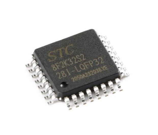
The first step in building an 8051 MCU minimum system circuit is selecting the appropriate microcontroller variant. While the original 8051 operated at 12MHz, modern derivatives from manufacturers like Atmel (now Microchip), NXP, Silicon Labs, and STMicroelectronics offer enhanced features including higher clock speeds, flash memory, lower power consumption, and additional peripherals. Popular choices include the AT89S52, P89V51RD2, and STC89C52RC, each offering different combinations of program memory, RAM, and special features. When selecting an 8051 variant, consider your application’s requirements for I/O pins, memory capacity, communication interfaces (UART, SPI, I2C), and power consumption.
The pin configuration of the 8051 is critical to understanding how to interface external components. The 8051 typically comes in a 40-pin DIP package or smaller surface-mount variants. Key pins for the minimum system include: - Power supply pins (VCC and GND): Provide operating voltage, typically +5V for classic variants or lower voltages for modern low-power versions - Reset pin (RST): Active-high input that initializes the microcontroller when pulled high - Oscillator pins (XTAL1 and XTAL2): Connect to external crystal or ceramic resonator - EA/VPP (External Access): Typically tied to VCC to indicate execution from internal program memory - Port 0, Port 1, Port 2, and Port 3: General-purpose I/O pins with various alternate functions
Understanding this pinout is essential because improper connections can prevent the microcontroller from functioning correctly or cause unreliable operation. For those seeking reliable components for their projects, platforms like ICGOODFIND offer comprehensive component databases and sourcing options that can simplify the selection process.
Clock Circuit Design and Implementation
The clock circuit serves as the heartbeat of the 8051 microcontroller, generating the precise timing references necessary for instruction execution and peripheral operations. A properly designed clock circuit is fundamental to system stability and performance. The most common approach uses a crystal oscillator connected between pins XTAL1 and XTAL2 with appropriate loading capacitors.
A typical crystal oscillator circuit consists of: - Quartz crystal: Determines the operating frequency (commonly 11.0592MHz for serial communication compatibility or 12MHz for general purposes) - Loading capacitors: Two ceramic capacitors (typically 22-33pF) connected from each crystal pin to ground - Internal oscillator circuitry: Already present within the microcontroller IC
The choice of crystal frequency involves important trade-offs. Higher frequencies enable faster execution but increase power consumption and electromagnetic interference. The peculiar value of 11.0592MHz is particularly useful when precise baud rates are needed for serial communication, as it allows generation of standard baud rates with minimal error. For applications where timing precision is less critical or board space is limited, ceramic resonators with built-in capacitors offer a compact alternative at slightly reduced accuracy.
Modern 8051 derivatives often include internal RC oscillators that eliminate external components entirely, saving board space and cost at the expense of frequency accuracy. Some variants even offer programmable internal oscillators with calibration registers to improve accuracy. When designing the PCB layout for the clock circuit, keep crystal traces as short as possible, away from noisy signals, and surrounded by a ground plane to minimize interference and ensure stable operation.
Reset Circuit Configuration and Power Management
The reset circuit provides a reliable method to initialize the 8051 microcontroller to a known state after power-up or during system malfunctions. Proper reset implementation ensures that the program execution begins consistently from address 0000H in program memory whenever conditions warrant a fresh start.
The most common reset configuration uses a simple RC network consisting of: - Electrolytic capacitor (typically 10-22μF): Provides time delay during power-up - Resistor (typically 8.2K-10KΩ): Limits current and provides discharge path - Manual reset switch: Optional push-button for user-initiated resets
During power-up, the capacitor initially appears as a short circuit, holding the RST pin high. As it charges through the resistor, the voltage at RST gradually decreases until it falls below the threshold level (approximately 1.2V for CMOS variants), completing the reset sequence. This power-on reset (POR) delay ensures that VCC has stabilized before the microcontroller begins program execution. The RC time constant (τ = R × C) should provide a reset pulse duration exceeding the manufacturer’s specified minimum (typically 2+ machine cycles).
For more critical applications where reliable operation under marginal power conditions is essential, dedicated reset supervisor ICs offer superior performance with precise voltage thresholds and built-in timing control. These devices monitor VCC continuously and assert reset automatically if voltage drops below a specified threshold (typically 4.5V for 5V systems), preventing erratic operation during brown-out conditions.
Power management in the minimum system extends beyond simple voltage regulation. Proper decoupling is crucial—place 100nF ceramic capacitors as close as possible to each VCC/GND pair on the microcontroller package, with additional bulk capacitance (10-47μF) near the power entry point. For modern low-power variants operating at 3.3V or lower voltages, ensure your voltage regulator can supply adequate current with minimal noise.
Advanced Considerations in Minimum System Design
Memory Interface Configurations
While many modern 8051 variants incorporate sufficient on-chip memory for most applications, understanding external memory interfacing remains important for more demanding projects or when working with classic 8051 chips with limited internal memory. The memory interface capability represents one of the distinctive features of the 8051 architecture.
The 8051 can address up to 64KB of external program memory (ROM) and 64KB of external data memory (RAM), accessed through different control signals: - PSEN (Program Store Enable): Activates when fetching instructions from external program memory - RD (Read) and WR (Write): Control data transfers with external data memory - ALE (Address Latch Enable): Demultiplexes the address/data bus
When external memory is used, Port 0 serves as a multiplexed address/data bus (AD0-AD7), requiring an external address latch (typically a 74HC373 or similar) to capture the address during ALE activation. Port 2 provides the higher address byte (A8-A15). This demultiplexing scheme allows the 16-bit address space with only 8 dedicated address pins.
For systems requiring both external program and data memory, careful PCB layout is essential—keep bus traces short and properly terminated to minimize signal integrity issues. Modern designs increasingly favor 8051 variants with sufficient on-chip flash memory to avoid external memory components altogether, simplifying board design and reducing component count.
Input/Output Port Configuration and Expansion
The four 8-bit bidirectional I/O ports (Port 0, Port 1, Port 2, and Port 3) provide interface capabilities to the outside world in an 8051 MCU minimum system circuit. Each port has distinct characteristics: - Port 0: Open-drain configuration requiring external pull-up resistors when used as general I/O - Ports 1-3: Feature internal pull-ups but may still benefit from external ones for heavier loads - Ports with alternate functions: Many pins serve dual purposes (serial communication, interrupts, timers)
Proper port configuration involves understanding both hardware connections and software initialization. All ports default as inputs after reset; software must configure them appropriately through the port latch registers. When driving LEDs or other modest loads directly from port pins, include appropriate series current-limiting resistors—the absolute maximum per-pin current typically ranges from 10-25mA depending on specific variants.
For applications requiring more I/O than available on the base microcontroller,port expansion techniques provide additional capabilities: - Standard ICs like the 8255 PPI offer additional programmable I/O lines - Serial-to-parallel converters (such as 74HC595) efficiently add outputs using few microcontroller pins - I2C or SPI-based GPIO expanders provide extensive expansion with simple interfaces
When designing with these expansion methods in mind,ICGOODFIND can be an invaluable resource for locating appropriate interface chips and understanding their implementation requirements.
System Reliability Enhancements
While a basic minimum system will function under ideal conditions,real-world applications demand additional considerations for reliable operation across varying environmental conditions and over extended periods.
Power supply design deserves particular attention—incorporate sufficient bulk capacitance near the voltage regulator input and output,and use low-ESR capacitors for digital circuits.Regulators with adequate current headroom(typically 50-100% beyond maximum expected draw)prevent voltage sag during peak demands.For noise-sensitive applications,linear regulators are preferable to switching types despite lower efficiency.
Implementing proper electrostatic discharge(ESD) protection on I/O lines connecting to external interfaces prevents damage from static electricity during handling or operation.TVS diodes or dedicated ESD protection ICs placed at connection points shunt harmful transient voltages before they reach sensitive microcontroller pins.
For systems operating in electrically noisy environments,electromagnetic compatibility(EMC) considerations become critical: - Use multilayer PCBs with dedicated ground planes - Implement proper trace spacing and routing techniques - Employ ferrite beads on power inputs and clock lines - Consider shielding for extremely noisy environments
Adding hardware watchdogs provides protection against software malfunctions—these independent timers require periodic servicing by the program;if not refreshed due to program errors,the watchdog triggers a system reset.Modern 8051 variants often include integrated watchdog timers requiring minimal external components.
Conclusion
The 8051 MCU minimum system circuit,while conceptually simple in its basic form,involves numerous considerations that significantly impact system performance,cost,and reliability.Mastering this fundamental configuration provides embedded systems designers with a solid foundation upon which increasingly sophisticated applications can be built.From selecting appropriate clock components to implementing robust reset circuits,and from configuring I/O ports to enhancing overall system reliability—each aspect contributes to creating an effective platform for embedded development.
Despite newer microcontroller architectures offering higher performance or lower power consumption,the enduring popularity of the 8051 family ensures its continued relevance across countless applications worldwide.The extensive code base,tool support,and accumulated design knowledge make it an excellent choice particularly for those new to embedded systems while still serving demanding industrial applications.Modern derivatives continue to enhance this classic architecture with contemporary features while maintaining backward compatibility.
As you embark on your next embedded project using this venerable architecture,a thorough understanding of these minimum system principles will serve you well.For those seeking reliable components,documentation,and implementation resources,ICGOODFIND offers comprehensive support that can streamline your development process.Whether you’re building your first blinking LED project or developing a sophisticated control system,the principles outlined here will help ensure your success with this remarkably resilient microcontroller family.


