


Recently, 3PEAK (a leading analog IC supplier) released the TPT29606 level-shifting chip designed specifically for I3C applications. This chip supports both Open-Drain and Push-Pull signal transmission, while being backward compatible with scenarios like I2C and SPI. With a minimum supply voltage of 0.72V and a maximum transmission rate of 26Mbps, it is widely applicable in fields such as servers, routers, storage devices, and PCs.

I. Four Core Advantages of the TPT29606
1. Ultra-Low Voltage Input, Low Power Consumption & High Reliability
The VCCA and VCCB pins of the TPT29606 support an input voltage as low as 0.72V, while the chip’s maximum withstand voltage reaches 2.5V. This design effectively reduces the risk of chip failure caused by input voltage overshoot, making it ideal for I3C or other applications requiring low-voltage level shifting.
More importantly, the chip’s quiescent current is only at the μA level. Even in long-term standby devices like servers or IoT equipment, it significantly reduces energy consumption, extending device battery life or lowering overall power costs.
2. Multi-Bus Compatibility & Industry-Leading Transmission Rates
Beyond meeting the level-shifting needs of I3C buses, the TPT29606 is backward compatible with the I2C protocol and also works with multiple common bus scenarios such as SPI, SMBus, and PMBus. This eliminates the need for separate component selection for different buses, simplifying the design process for engineers.
In terms of speed performance, the chip is optimized for different buses: it supports a maximum transmission rate of 12.5MHz for I3C bus applications (meeting high-speed interconnection needs of sensors and peripherals) and an even higher rate of 26Mbps for SPI bus applications (suitable for storage devices, FPGAs, and other scenarios requiring strict speed requirements).
3. Electrical Isolation + Automatic Direction Detection for Easier Design
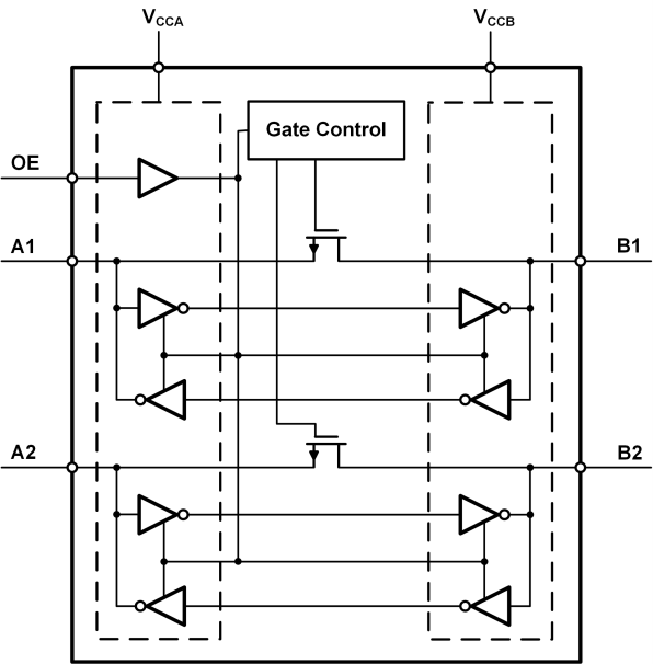
When the chip’s enable pin (OE) or any VCCx channel is at low level, all I/O pins immediately enter a high-impedance state, achieving electrical isolation between the two ends of the chip. This function prevents signal interference when the device is powered off or in an abnormal state, protecting the safety of upstream and downstream circuits.
Additionally, the TPT29606 has no strict power-up sequence requirements for VCCA and VCCB. During operation, it can also automatically detect the signal transmission direction and switch accordingly—no additional direction control pins or circuits are needed. This not only reduces PCB wiring space but also lowers system design complexity and shortens development cycles.
4. High ESD and Latch-Up Capabilities to Enhance System Robustness
The TPT29606 excels in anti-interference and stability:
- Its HBM (Human-Body Model, compliant with ANSI/ESDA/JEDEC JS-001) reaches ±7kV,
- CDM (Charged-Device Model, compliant with ANSI/ESDA/JEDEC JS-002) reaches ±1.5kV,
- Latch-up (compliant with JESD78) capability is as high as ±600mA.
These features can withstand electrostatic shocks during production, transportation, and use, and prevent chip damage from excessive current during circuit abnormalities—significantly improving the reliability of customers’ end systems.

II. Key Specifications of the TPT29606
- Applicable Scenarios: Fully covers level-shifting needs for buses like I3C, I2C, SPI, SMBus, and PMBus; suitable for consumer electronics, industrial control, and network equipment.
- Number of Channels: 2 channels (dual-channel design), enabling simultaneous processing of two signal conversion paths to improve single-chip utilization.
- Input Voltage Range: Both VCCA and VCCB support 0.72~1.98V (VCCA ≤ VCCB required), adapting to low-voltage power supply systems.
- Operating Temperature Range: -40℃ ~ 125℃, capable of withstanding harsh high/low-temperature industrial environments and compatible with automotive electronics and outdoor equipment.
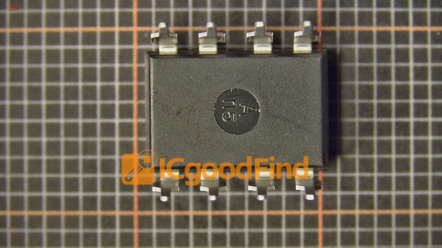
- Package Types: Offers SOT23-8 (thin, small package for space-constrained PCB layouts) and DFN1.4×1-8 (ultra-small package for miniaturized devices), meeting packaging needs of different products.
III. Typical Applications & Circuit Design Highlights of the TPT29606
The TPT29606’s internal circuit design is optimized for multi-bus scenarios, with a core highlight being its rising/falling edge acceleration circuit: When a signal rising edge is detected, the chip’s internal monostable circuit triggers the acceleration circuit to activate, quickly pulling the bus voltage up to VCCX to avoid signal delay or distortion. After the rising edge acceleration circuit turns off, the bus maintains a high level through an internal 10kΩ pull-up resistor.
Notably, this internal pull-up resistor is only activated when "both VCCA and VCCB are powered on, OE is at high level, and the bus is at high level"—it is automatically disabled during low-level periods. This design further reduces chip power consumption, making it ideal for battery-powered devices.
In different bus applications, the chip’s usage details vary slightly:
- I3C Applications: No additional external pull-up resistors are needed; the internal resistor can be used directly, simplifying circuit design.
- I2C Applications: External pull-up resistors must be retained to ensure the bus meets I2C protocol voltage requirements.
Additionally, the chip features automatic power-down protection: If either VCCA or VCCB is disconnected, the chip immediately enters power-down mode and shuts down all output interfaces, preventing damage to external circuits due to abnormal power supply. For enable control, the OE pin can be flexibly configured—it can be directly connected to VCCA when no control is needed, or to a GPIO when manual control is required, adapting to the control needs of different systems.
ICgoodFind’s Perspective
ICgoodFind is deeply rooted in the semiconductor supply chain and has established a stable cooperation with 3PEAK. We can provide customers with spot supply and customized BOM matching services for the TPT29606 chip. The low-voltage compatibility and multi-bus adaptability of this chip effectively address level-shifting pain points in servers, PCs, and storage devices. Leveraging our partnerships with original manufacturers, we will help customers quickly access samples and mass-production resources, accelerating product development and market launch.


