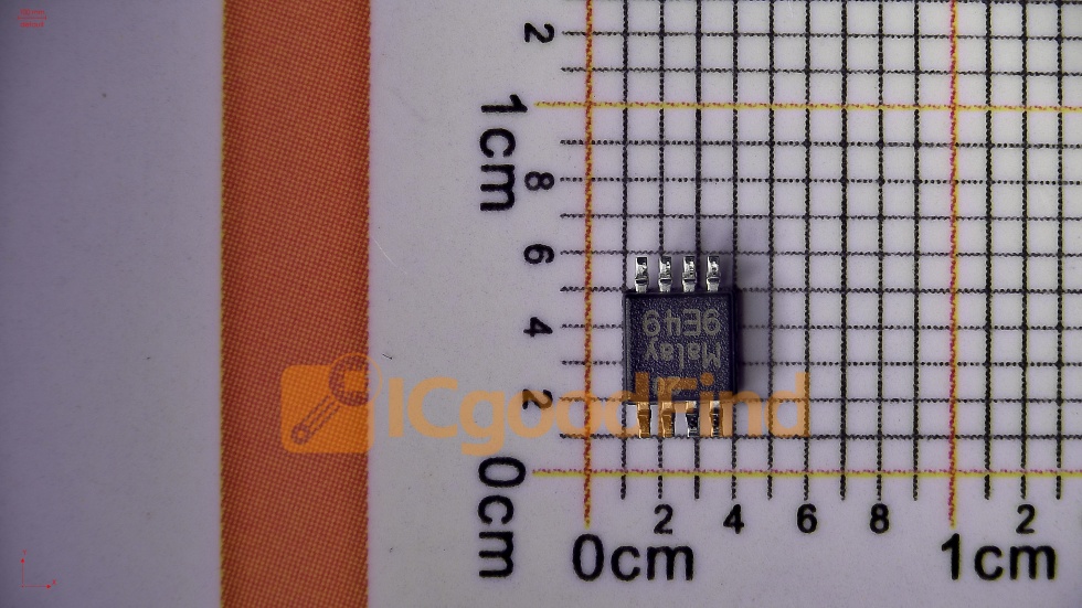
STM32G030F6P6TR: The Compact Powerhouse for Cost-Sensitive Embedded Designs
Introduction
In the rapidly evolving world of embedded systems, engineers constantly face a delicate balancing act between performance, power consumption, and bill-of-materials (BOM) cost. While high-end microcontrollers often steal the spotlight, the real workhorses of millions of industrial and consumer products are the humble, cost-effective MCUs that deliver reliable performance without breaking the bank. The STM32G030F6P6TR from STMicroelectronics is precisely such a device—a compact, feature-rich, and remarkably affordable 32-bit microcontroller designed for high-volume, space-constrained applications. Whether you are designing a smart sensor node, a motor controller, or a simple IoT endpoint, this chip offers an impressive blend of Arm® Cortex®-M0+ efficiency, robust analog peripherals, and a tiny footprint. In this article, we will dive deep into the architecture, key features, and practical applications of the STM32G030F6P6TR, and explain why it deserves a prime spot on your next design’s BOM. For sourcing this part and comparing real-time availability, ICGOODFIND is an excellent platform to check stock and pricing across global distributors.
Main Body
Part 1: Core Architecture and Processing Efficiency
At the heart of the STM32G030F6P6TR lies a 32-bit Arm® Cortex®-M0+ processor running at up to 64 MHz. This may sound modest compared to Cortex-M4 or M7 parts, but for a vast array of control and monitoring tasks, it is more than sufficient. The M0+ core is renowned for its exceptional energy efficiency, requiring fewer clock cycles per instruction than older 8-bit or 16-bit architectures while offering a true 32-bit address space and processing power.
Memory configuration is another critical aspect. This specific variant comes with 32 KB of Flash memory and 8 KB of SRAM. While not massive, this is ideal for firmware that handles sensor reading, simple control loops, and communication protocols. The Flash memory supports up to 10,000 write/erase cycles, ensuring robust endurance for applications that require in-field firmware updates. The SRAM, though compact, is sufficient for stack operations, dynamic buffers, and small data arrays. For designs that need more headroom, the G0 series offers larger variants, but the F6P6TR strikes a sweet spot for cost-optimized projects.
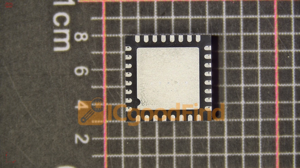
Clock management is also a highlight. The STM32G030F6P6TR integrates an internal 16 MHz RC oscillator (HSI) that can be calibrated to achieve better accuracy, plus an internal 32 kHz RC oscillator (LSI) for low-power wake-up and watchdog operations. This eliminates the need for external crystals in many applications, reducing component count and PCB space. For applications requiring precise timing, the device also supports an external crystal oscillator (HSE) up to 32 MHz. The clock tree is flexible, allowing peripheral clocks to be divided down to save power, which is crucial for battery-operated devices.
Power consumption is where the M0+ core truly shines. The STM32G030F6P6TR offers multiple low-power modes: Sleep, Stop, and Standby. In Stop mode, the device can wake up from external interrupts or the RTC, consuming as little as a few microamps. This makes it an excellent choice for battery-powered wireless sensors that need to sleep for 99% of their operational life. Additionally, the device operates over a wide voltage range of 2.0V to 3.6V, simplifying power supply design and allowing direct connection to standard 3.3V logic and analog sensors.
Part 2: Rich Peripheral Set and Analog Integration
Despite its low cost and small package, the STM32G030F6P6TR does not skimp on peripherals. It is housed in a TSSOP20 package (hence the “F6P6” designation), which measures just 6.4mm x 4.4mm—small enough for compact PCBs but still hand-solderable for prototyping. Within this tiny package, the chip packs a surprising number of features.
Analog capabilities are a standout. The device includes a 12-bit ADC with up to 16 channels (though the number of external pins limits simultaneous usage). This ADC supports hardware oversampling, which can effectively increase resolution to 16 bits for low-frequency signals, and features a fast conversion time of up to 2.4 µs. This is perfect for reading thermistors, potentiometers, current sense resistors, or even simple audio envelope detection. The ADC also includes a built-in internal reference voltage and a temperature sensor, eliminating the need for external reference ICs in many designs.
Timers are another strong suit. The STM32G030F6P6TR includes one advanced 16-bit timer (TIM1) with complementary PWM outputs and dead-time insertion, making it ideal for motor control (BLDC or PMSM) and power conversion (buck/boost converters). It also has two general-purpose 16-bit timers (TIM3, TIM14) and a basic timer (TIM6) for time-base generation. The advanced timer can generate up to 6 independent PWM channels, giving designers flexibility for multi-phase control.
Communication interfaces are well covered for a budget MCU. The device features: - Two I2C interfaces (one supporting SMBus/PMBus) - Two USARTs (one with full modem control and hardware flow control) - One SPI (with I2S capability)
These interfaces allow the chip to talk to a wide range of external components: EEPROMs, OLED displays, SD cards, GPS modules, LoRa radios, and more. The USARTs support DMA (Direct Memory Access) , which offloads the CPU from byte-by-byte data transfer, freeing processing power for other tasks. The I2C interface runs at up to 1 MHz in Fast Mode Plus, enabling high-speed sensor polling.
Other notable peripherals include a DMA controller with 5 channels, a CRC calculation unit (useful for data integrity checks), a real-time clock (RTC) with calendar and alarm functions, and a window watchdog and independent watchdog for system reliability. The GPIO pins are 5V-tolerant, allowing direct connection to legacy 5V logic without level shifters—a significant cost and space saver.
Part 3: Practical Applications and Development Ecosystem
The STM32G030F6P6TR is not just a theoretical marvel; it is designed for real-world, high-volume applications. Let’s explore three typical use cases that highlight its versatility.
Application 1: Smart Home Sensors and Controllers In a smart thermostat or a PIR motion sensor, the MCU needs to wake up periodically, read a temperature/humidity sensor (e.g., SHT30) via I2C, process the data, and send it to a central hub via RF (e.g., Zigbee or Sub-GHz). The STM32G030F6P6TR excels here. Its Stop mode with RTC wake-up allows the device to sleep for 10 seconds, consume only 3 µA, then wake up, perform a 5 ms burst of activity, and go back to sleep. The 12-bit ADC reads the analog output of a photodiode or a gas sensor, while the USART communicates with a Wi-Fi module (e.g., ESP-01) for cloud connectivity. The small TSSOP20 package fits neatly into a compact PCB that can be placed inside a wall switch or a smoke detector housing.
Application 2: Low-Cost Motor Control For a small DC fan, a water pump, or a toy car, the STM32G030F6P6TR provides the necessary PWM and timer features. The TIM1 advanced timer generates complementary PWM signals with programmable dead-time, driving a half-bridge or full-bridge MOSFET driver. The ADC reads the current sense resistor voltage to implement simple overcurrent protection or closed-loop speed control. The 64 MHz clock ensures fast control loop execution (e.g., 20 kHz PWM frequency with 10-bit resolution). The device’s robust I/O structure can directly drive the gate driver ICs, and its wide operating voltage range allows it to be powered from a 3.7V Li-ion battery or a 5V USB supply with a simple LDO.
Application 3: Industrial Sensor Node with RS-485 In industrial automation, sensor nodes often communicate over long distances using RS-485. The STM32G030F6P6TR’s USART with hardware flow control and DMA can efficiently manage the RS-485 transceiver (e.g., MAX485). The device reads a 4-20 mA current loop signal using the ADC, linearizes the data in firmware, and transmits it over the bus. The CRC unit ensures data packet integrity, while the independent watchdog resets the system in case of a firmware hang. The wide temperature range (-40°C to +85°C) makes it suitable for harsh factory floors.
Development Ecosystem and Sourcing STMicroelectronics provides a comprehensive STM32CubeG0 software package, which includes the HAL (Hardware Abstraction Layer), low-layer drivers, and middleware (e.g., USB PD, Touch Sensing). The STM32CubeMX graphical tool allows you to configure pins, clocks, and peripherals in minutes, generating initialization C code. For debugging, the SWD (Serial Wire Debug) interface requires only two pins, and cheap ST-Link clones are widely available. The device is also supported by Arduino IDE via the STM32duino core, making it accessible to hobbyists and rapid prototyping.
When it comes to purchasing, the “TR” suffix in the part number indicates tape-and-reel packaging, which is ideal for automated SMT assembly. However, for small quantities or prototyping, you can also find it in tube packaging. To ensure you get genuine parts at competitive prices, ICGOODFIND is a reliable online platform that aggregates inventory from authorized distributors like Mouser, Digi-Key, and Arrow. It allows you to compare prices, check lead times, and filter by packaging and quantity, saving you hours of manual searching.
Conclusion
The STM32G030F6P6TR is a testament to the fact that high performance doesn’t always require a high budget. By combining the efficient Arm Cortex-M0+ core with a rich set of analog and digital peripherals, a wide operating voltage range, and multiple low-power modes, this microcontroller delivers exceptional value for a broad spectrum of embedded applications. Its TSSOP20 package is ideal for space-constrained designs, while its 32 KB Flash and 8 KB SRAM are perfectly suited for focused firmware tasks. From smart home sensors to industrial motor control, this chip proves that you don’t need a high-end MCU to build a smart, reliable, and cost-effective product.

For engineers and procurement specialists alike, the key takeaway is that the STM32G030F6P6TR offers a seamless migration path within the STM32G0 family—if your project outgrows this variant, you can move to a larger Flash/SRAM version without rewriting your code. The mature STM32Cube ecosystem, extensive community support, and long-term availability from STMicroelectronics ensure that your design will remain manufacturable for years to come. When you are ready to source this part, remember to check ICGOODFIND for real-time stock levels and competitive pricing across multiple distributors. In a world where every cent counts, this little MCU is a giant leap forward in cost-effective embedded design.