
TSMC is reportedly in negotiations to acquire AUO’s L7 (7.5‑gen) and L5C (5‑gen) panel fabs in the Central Taiwan Science Park, with a deal value estimated at over NT$30B (~$210M) – a record for older panel fab transactions in the region. The sites would be converted for advanced packaging capacity expansion, following the model pioneered by Innolux’s transition to semiconductor back-end services.
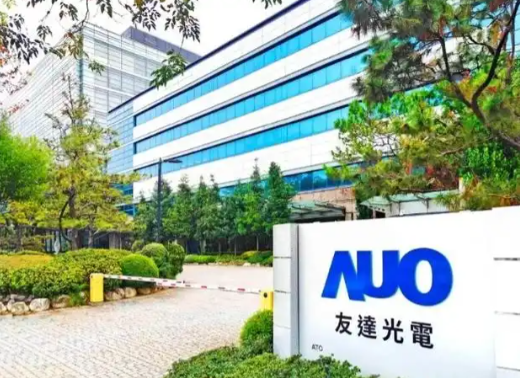
The two fabs sit next to TSMC’s existing Zhongke 15 campus, offering ready‑to‑use cleanroom space and power allocation – scarce assets for packaging expansion. TSMC aims to leverage AUO’s mature glass substrate know‑how to deploy FOPLP (fan‑out panel‑level packaging) and CoPoS technologies, bridging front‑end fabrication with on‑site packaging.
CoPoS is positioned as TSMC’s next‑gen 2.5D packaging platform after CoWoS. Large AI chips suffer from material waste, cost, and warpage on circular 300mm wafers – glass panel substrates (e.g., 310mm × 310mm) solve these issues. TSMC’s first CoPoS pilot line at Chiayi is already in equipment debug and material validation, with roughly one year needed to stabilize yields.
Panel fabs offer large‑area cleanrooms and substrate‑handling experience – operational know‑how critical for panel‑level packaging ramp. Both TSMC and ASE are aggressively hunting for industrial sites with stable power. Many panel makers are repurposing idle lines to capture AI packaging margins.
TSMC declined to comment on market rumors; AUO also said it does not respond to speculation.
ICgoodFind Take:
Old fabs, new purpose. Panel‑level glass packaging is no longer theoretical – TSMC’s fab hunt confirms it. For procurement, watch for glass substrate and large‑panel equipment suppliers – this shifts the packaging supply base from wafer‑centric to panel‑scale.