

Shanghai Xinshang Microelectronics Equipment has secured repeat volume orders for its self-developed AST6200 350nm stepper projection lithography tool, after passing process validation at a domestic compound semiconductor leader. The system was first delivered for testing in November 2025 and is now commercially deployed.
The AST6200 supports power devices, RF front-end chips, optoelectronics, and Micro-LED displays – covering Si, SiC, GaN, GaAs, InP, and sapphire wafers (2‑ to 8‑inch). Key capabilities: 350nm resolution with multi‑mode illumination, high‑precision alignment for overlay accuracy, high‑intensity exposure source, and fast wafer handling – all driving yield and cost efficiency.
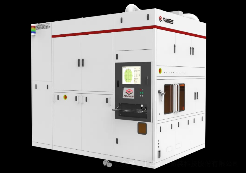
Custom focus/leveling and edge/backside alignment options handle transparent, semi‑transparent, and stepped substrates, plus bonded wafer alignment. One tool supports multiple product lines with flexible recipe switching.
Full‑stack software – from driver to process control – is developed in‑house, with remote O&M and expansion headroom for smart fab integration.
Xinshang (founded Feb 2025) also offers packaging steppers, laser annealers, and wafer inspection systems. Its team holds patents in projection optics, precision stages, and exposure modules – positioning itself as a domestic alternative for critical lithography components.
ICgoodFind Take:
Repeat orders from a Tier‑1 compound fab are the real validation. This isn't a lab demo – it's production‑ready 350nm steppers with local software and service. For procurement, this adds a credible domestic source for GaN/SiC lithography – watch for capacity expansion and follow‑on tools in 2027.