


Multilayer PCB Board Used Integrated Circuits: The Backbone of Modern Electronics
Introduction
In the rapidly evolving world of electronics, the demand for higher performance, miniaturization, and reliable signal integrity has never been greater. At the heart of this technological revolution lies the multilayer PCB board used integrated circuits — a sophisticated combination of printed circuit board (PCB) technology and advanced integrated circuits (ICs). These boards are no longer just simple substrates for mounting components; they are complex, multi-layered structures that enable the seamless integration of hundreds or even thousands of ICs in a compact form factor. From smartphones and medical devices to aerospace systems and 5G infrastructure, the multilayer PCB board used integrated circuits is the unsung hero that makes modern electronics possible. This article explores the design principles, manufacturing challenges, and application advantages of these critical components, while also highlighting how platforms like ICGOODFIND are revolutionizing the sourcing of high-quality multilayer PCBs and ICs for engineers and manufacturers worldwide.
Part 1: Understanding the Architecture of Multilayer PCB Boards Used Integrated Circuits
1.1 What Makes a Multilayer PCB Different?
A multilayer PCB board used integrated circuits is defined by its stacked structure of multiple conductive layers separated by insulating dielectric materials. Unlike single-layer or double-layer boards, these PCBs typically consist of 4 to 40 layers, each serving a specific purpose. The key components include:
- Signal layers: Carry high-speed digital or analog signals between ICs.
- Power planes: Distribute stable voltage levels across the board.
- Ground planes: Provide low-impedance return paths and reduce electromagnetic interference (EMI).
- Buried and blind vias: Connect specific layers without penetrating the entire board, saving space and improving signal quality.
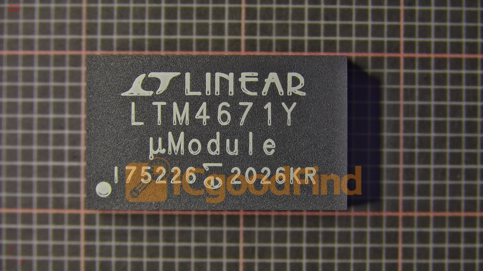
The integrated circuits mounted on these boards — such as microprocessors, memory chips, FPGAs, and RF ICs — require precise impedance control, thermal management, and minimal crosstalk. A well-designed multilayer PCB achieves this by carefully stacking layers and routing traces to match the ICs’ electrical requirements.
1.2 The Role of Layer Count in IC Performance
The number of layers in a multilayer PCB board used integrated circuits directly impacts the density and performance of the final product. For example:
- 4-layer boards: Common in consumer electronics like IoT devices, where cost and space are constrained.
- 6 to 8-layer boards: Used in mid-range applications like automotive electronics and industrial controllers, offering better signal isolation.
- 12 to 20+ layers: Essential for high-speed computing, telecommunications, and medical imaging equipment, where signal integrity and power distribution are critical.
Each additional layer allows for dedicated power and ground planes, which reduce noise and improve signal quality. However, increasing layer count also raises manufacturing complexity and cost. Engineers must balance these factors when designing a multilayer PCB board used integrated circuits for a specific application.
1.3 Material Selection for High-Frequency ICs
The dielectric materials used in multilayer PCBs significantly affect the performance of integrated circuits. For high-frequency ICs (e.g., RF amplifiers, radar systems), materials like Rogers 4003C or PTFE-based laminates are preferred due to their low dielectric loss and stable dielectric constant. In contrast, FR-4 remains the most cost-effective choice for general-purpose applications, but its performance degrades at frequencies above 1 GHz.
When sourcing materials for a multilayer PCB board used integrated circuits, platforms like ICGOODFIND provide engineers with detailed specifications and certified suppliers, ensuring that the chosen materials meet the thermal, electrical, and mechanical demands of the ICs.
Part 2: Design and Manufacturing Challenges of Multilayer PCBs for ICs
2.1 Signal Integrity and Impedance Matching
One of the most critical challenges in designing a multilayer PCB board used integrated circuits is maintaining signal integrity. High-speed ICs generate fast rise times and high-frequency harmonics, which can cause reflections, ringing, and crosstalk if not properly managed. Key design techniques include:
- Controlled impedance traces: Matching the characteristic impedance of the PCB trace to the IC’s output impedance (typically 50Ω or 100Ω differential).
- Differential pair routing: Used for high-speed data interfaces like USB, HDMI, and PCIe, where two traces carry opposite signals to cancel noise.
- Via optimization: Minimizing via stubs and using back-drilling to reduce parasitic capacitance and inductance.
Simulation tools are essential for predicting signal behavior before fabrication. Engineers use software like Altium Designer or Cadence Allegro to model the multilayer PCB board used integrated circuits and verify that timing margins and eye diagrams meet IC specifications.
2.2 Thermal Management in Dense IC Layouts
Modern integrated circuits, especially high-power processors and power management ICs, generate significant heat. In a multilayer PCB board used integrated circuits, heat must be dissipated efficiently to prevent thermal runaway and performance degradation. Solutions include:
- Thermal vias: Arrays of vias that transfer heat from ICs to internal copper planes or external heat sinks.
- Copper coin inserts: Solid copper blocks embedded in the PCB to spread heat laterally.
- Metal-core PCBs: Using aluminum or copper as the base layer for extreme thermal requirements.
ICGOODFIND offers a wide range of thermal management components and PCB substrates specifically designed for high-power ICs, helping engineers select the right materials for their multilayer PCB board used integrated circuits.
2.3 Manufacturing Precision and Yield
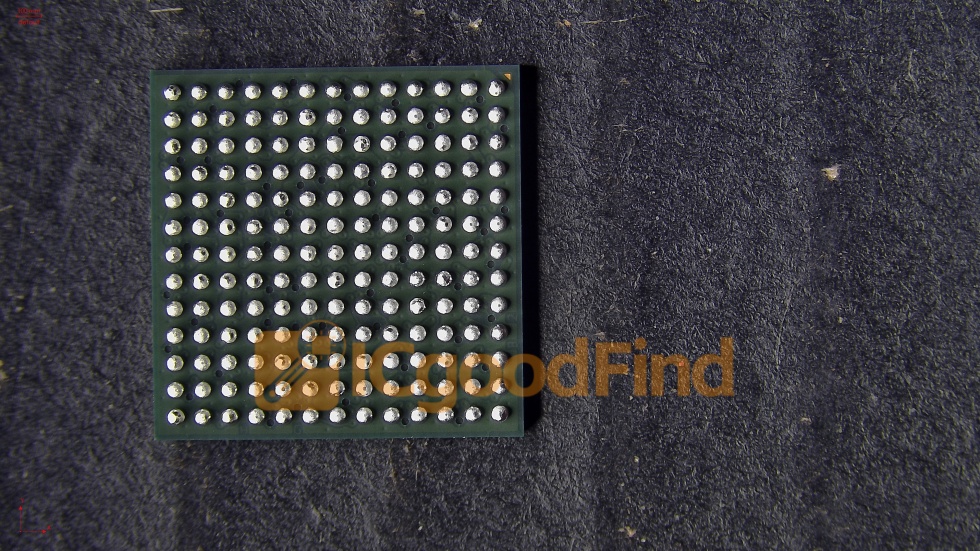
Producing a multilayer PCB board used integrated circuits requires extreme precision in layer alignment, etching, and drilling. Even a micron-level misalignment can cause short circuits or open circuits in dense IC packages like BGA (Ball Grid Array) or QFN (Quad Flat No-lead). Key manufacturing steps include:
- Lamination: Bonding multiple layers under high temperature and pressure, ensuring uniform thickness and void-free adhesion.
- Laser drilling: Creating micro-vias with diameters as small as 50 microns for high-density interconnect (HDI) designs.
- Plating: Depositing copper in vias and through-holes to ensure reliable electrical connections.
Quality control is paramount. Manufacturers perform automated optical inspection (AOI) , X-ray inspection, and electrical testing to verify that each multilayer PCB board used integrated circuits meets the IPC-6012 or IPC-6018 standards. Platforms like ICGOODFIND connect buyers with ISO-certified manufacturers who specialize in high-reliability multilayer PCBs for IC applications.
Part 3: Applications and Advantages of Multilayer PCBs with Integrated Circuits
3.1 Consumer Electronics: Smartphones and Wearables
The multilayer PCB board used integrated circuits is the backbone of modern smartphones, which contain over 20 layers to accommodate application processors, memory ICs, RF transceivers, and power management units. The advantages include:
- Space savings: Multiple layers allow for component stacking and fine-pitch routing, enabling ultra-thin designs.
- EMI shielding: Dedicated ground planes and buried capacitors reduce interference between the cellular modem and the display driver.
- Battery efficiency: Optimized power planes minimize voltage drops, extending battery life.
For wearable devices like smartwatches, flexible multilayer PCBs are often used, combining rigid sections for ICs with flexible sections for sensors and displays. ICGOODFIND provides access to flex-rigid PCB manufacturers that specialize in multilayer board used integrated circuits for compact, lightweight designs.
3.2 Automotive Electronics: ADAS and Infotainment
The automotive industry relies heavily on multilayer PCB board used integrated circuits for Advanced Driver-Assistance Systems (ADAS) , infotainment systems, and electric vehicle (EV) powertrains. These boards must withstand extreme temperatures (-40°C to +150°C), vibration, and electromagnetic interference. Key features include:
- Thick copper layers: For high-current handling in motor controllers and battery management systems.
- High-Tg materials: Glass transition temperatures above 170°C to prevent delamination.
- Redundant routing: For safety-critical ICs, ensuring fail-safe operation.
ICGOODFIND offers automotive-grade multilayer PCBs that comply with AEC-Q100 and ISO 26262 standards, ensuring reliability in harsh environments.
3.3 Telecommunications and 5G Infrastructure
5G base stations and network equipment demand multilayer PCB board used integrated circuits with extremely low signal loss and high power handling. These boards often feature:
- Low-loss laminates: Such as Megtron 6 or RO3003, with dielectric constants below 3.5.
- Hybrid stackups: Combining different materials to optimize cost and performance for RF and digital ICs.
- Embedded passive components: Resistors and capacitors integrated into the PCB layers to reduce parasitic effects.
The high layer count (up to 40 layers) in these boards enables complex routing for massive MIMO antennas and beamforming ICs. ICGOODFIND helps engineers source high-frequency PCB materials and certified manufacturers for 5G applications.
Conclusion
The multilayer PCB board used integrated circuits represents a pinnacle of engineering achievement, enabling the miniaturization, performance, and reliability demanded by today’s electronic devices. From the architectural design of signal and power layers to the manufacturing precision required for high-density IC packages, every aspect of these boards is optimized for signal integrity, thermal management, and cost efficiency. As technology advances toward 6G communications, autonomous vehicles, and AI-driven systems, the role of multilayer PCBs will only grow more critical.
For engineers and procurement professionals seeking to source high-quality multilayer PCBs and integrated circuits, ICGOODFIND stands out as a trusted platform. It offers verified suppliers, detailed technical specifications, and competitive pricing for a wide range of multilayer PCB board used integrated circuits — from prototype runs to high-volume production. By leveraging ICGOODFIND, you can accelerate your design cycle, reduce risk, and ensure that your next product meets the highest standards of performance and reliability.