


Japanese printing giant Dai Nippon Printing Co., Ltd. (DNP) has announced a significant breakthrough in chip manufacturing technology, developing a Nanoimprint Lithography (NIL) process capable of 10-nanometer circuit patterning. This achievement is equivalent to patterning logic semiconductors at the 1.4nm-class level, positioning NIL as a potential alternative to the dominant but expensive Extreme Ultraviolet (EUV) lithography.

While EUV lithography is essential for cutting-edge chips, its extremely high investment cost and energy consumption pose significant barriers, especially for smaller manufacturers. DNP's NIL technology, refined over two decades of development, offers a simpler "stamping" process that directly imprints circuit patterns onto substrates. The company claims this method uses only about 1/10th of the exposure energy of mainstream processes and can drastically reduce equipment and manufacturing costs.

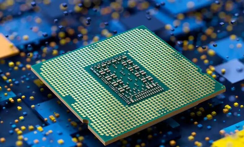
The core value of the 10nm NIL technology lies in its potential to replace EUV in certain manufacturing steps, providing an advanced process option for fabs that cannot afford multi-hundred-million-dollar EUV tools. The technology targets the miniaturization needs of advanced logic chips for smartphones and data centers. DNP has begun customer evaluations and plans to complete verification and establish a mass production system by 2027, with a goal of generating 4 billion yen in related revenue by fiscal 2030.
ICgoodFind's Insight
DNP's successful development of a 10nm NIL process introduces a credible, cost-disruptive competitor in the advanced patterning space. If commercialized successfully, it could diversify the supply chain, reduce entry barriers for advanced node manufacturing, and reshape the global cost structure for leading-edge chip production.


