
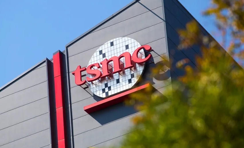
TSMC has received the construction permit for its A14 fab in Taichung, clearing the way for its massive $49 billion investment in advanced manufacturing. The new facility will focus on the development and production of 1.4-nanometer chips, with mass production scheduled to begin in the second half of 2028.

The 1.4nm process represents a significant leap from the 2nm node, offering a 15% speed gain at the same power or a 25-30% power reduction at the same performance. It also increases logic density by 20-23%, promising major efficiency improvements for high-performance computing and AI accelerators. A key technical achievement is that the node is designed to achieve its targets without relying on High-NA EUV lithography, thereby mitigating equipment risks and costs.
This strategic move positions TSMC to capture the entire market for the most advanced semiconductor technology starting in 2028, further solidifying its industry leadership.
ICgoodFind : TSMC's 1.4nm fab is set to reshape the semiconductor landscape, with its technical breakthroughs poised to upgrade the supply of high-end chips for the global tech ecosystem.