

FSMC Drives SDRAM: A Comprehensive Guide to High-Speed Memory Interface on Microcontrollers
Introduction
In the realm of embedded systems and high-performance microcontroller applications, efficient memory expansion is often a critical requirement. As applications grow more complex—demanding higher-resolution graphics, larger data buffers, or real-time signal processing—the internal memory of a microcontroller (MCU) can quickly become a bottleneck. This is where external memory interfaces come into play, and one of the most powerful and flexible solutions for ARM Cortex-M based microcontrollers, particularly those from STMicroelectronics, is the Flexible Static Memory Controller (FSMC). This article delves deep into how the FSMC drives SDRAM, unlocking significant performance gains for memory-intensive designs. We will explore the technical foundations, configuration intricacies, and practical advantages of this interface, highlighting why it remains a cornerstone for developers pushing the boundaries of embedded capabilities. For engineers seeking specialized components and in-depth technical resources to implement such solutions, platforms like ICGOODFIND provide invaluable access to a curated selection of memory chips and controller ICs.
Part 1: Understanding FSMC and Its Role in Memory Expansion
The Flexible Static Memory Controller (FSMC) is a sophisticated peripheral integrated into many mid-to-high-end STM32 microcontrollers. As its name implies, it was initially designed to interface with various types of static memories, such as SRAM, NOR Flash, PSRAM, and even LCD parallel interfaces. Its flexibility stems from its bank-based architecture, where different memory types can be mapped to different banks with individually configurable timing parameters.
However, the true power of FSMC in some advanced MCU families (like the STM32F2, F4, F7, and H7 series) extends beyond static memories. Through specific configurations and supported modes, it can also interface with dynamic memories, most notably Synchronous DRAM (SDRAM). SDRAM offers a compelling advantage: very high density at a relatively low cost per megabyte. This makes it ideal for applications requiring large frame buffers (e.g., TFT displays), audio sample storage, or complex algorithm data sets.

The FSMC acts as the crucial bridge between the MCU’s internal high-speed bus and the external SDRAM device. It handles the complex protocol required by SDRAM, including: * Bank Management: SDRAM is internally divided into multiple banks to allow overlapping operations. * Row/Column Addressing: It manages the multiplexing of address lines to specify row and column addresses. * Refresh Control: It automatically generates the necessary refresh commands to maintain data integrity in the DRAM cells. * Timing Generation: It controls critical delays like Row Address Strobe (RAS) to Column Address Strobe (CAS) delay (tRCD), CAS Latency (CL), and write/read recovery times.
By offloading these tasks to dedicated hardware, the FSMC frees up the CPU core from low-level memory protocol management, allowing it to focus on application logic while maintaining high-speed data throughput.
Part 2: Technical Deep Dive: Configuring FSMC for SDRAM
Successfully driving SDRAM with the FSMC requires meticulous hardware design and software configuration. The process is more involved than interfacing with static memory due to SDRAM’s initialization sequence and refresh requirements.
Hardware Considerations: The connection involves mapping MCU pins to the FSMC’s SDRAM bank (typically Bank 1 or 2). Key signal groups include: * Address Bus (A0-Ax & RAx): For row/column addressing. * Data Bus (D0-D15/D31): Width is configurable (16-bit or 32-bit). * Control Signals: These are critical and include: * SDCKE: Clock Enable. * SDCLK: Clock output from FSMC to SDRAM. * SDNE: Chip Select. * NRAS: Row Address Strobe. * NCAS: Column Address Strobe. * NWE: Write Enable. * NBL[1:0]: Byte Lane masks for 16⁄32-bit access. Proper PCB layout is essential here. Signal integrity for SDCLK and address/data lines must be prioritized with controlled impedance, matched lengths for critical traces, and appropriate termination to prevent reflections that could corrupt data.
Software Configuration Sequence: The initialization in firmware is a multi-step process that must follow the SDRAM device’s datasheet precisely. The core steps involve:
- FSMC Clock Enable: Enable the FSMC and GPIO clocks in the RCC registers.
- GPIO Configuration: Set all related pins to alternate function mode for FSMC with appropriate speed (high speed).
- FSMC Timing Parameters: Configure the FSMC_SDCR (Control Register) and FSMC_SDTR (Timing Register). This is where developers spend significant time tuning for stability and performance. Key parameters include:
- CAS Latency: The number of clock cycles between a read command and data availability.
- Row Precharge Delay (tRP): Time to close one row and open another.
- Row-to-Column Delay (tRCD): Delay from activating a row to issuing a read/write command.
- Row Cycle Time (tRC): Minimum time between successive active commands to the same bank.
- SDRAM Initialization Sequence: This is sent via command mode. The FSMC must issue a series of specific commands in order:
- Send a Clock Configuration Enable command.
- Wait for a minimum period (typically >100µs).
- Issue an All Bank Precharge command.
- Perform multiple Auto Refresh commands (usually 2-8 cycles).
- Set the Mode Register to define burst length, CAS latency, and operating mode.
- Finally, set the Refresh Rate in the FSMC_SDRTR register based on the SDRAM’s refresh requirement and system clock.
Once initialized, the SDRAM memory space appears as a contiguous block in the MCU’s address map. The CPU or DMA controller can then read from or write to it using simple pointer accesses, with the FSMC handling all background protocol tasks seamlessly.
Part 3: Advantages, Challenges, and Best Practices
Leveraging FSMC to drive SDRAM brings transformative benefits but also introduces specific challenges that engineers must navigate.
Key Advantages: * Massive Memory Expansion: Enables adding up to several hundreds of megabytes of RAM, far exceeding internal SRAM limits. * High Performance: With proper configuration, the interface can support full-speed synchronous access, maximizing bandwidth for data-intensive tasks. * Hardware Abstraction: The complexity of SDRAM timing is managed by hardware, simplifying software development after initial setup. * Direct Memory Access (DMA) Compatibility: The memory region is directly accessible by DMA controllers, enabling zero-CPU-overhead data transfers between peripherals (like camera sensors or Ethernet) and SDRAM.
Common Challenges and Solutions: * Complex Initialization: A single mistimed parameter can lead to silent data corruption. Solution: Use vendor-provided HAL libraries or low-level drivers as a reliable starting point and validate against the SDRAM datasheet. * Signal Integrity Issues: At higher clock speeds (>50MHz), poor layout causes failures. Solution: Adhere strictly to MCU reference board layouts, use short traces, and consider on-board termination resistors. * Power Consumption: SDRAM requires periodic refresh even in low-power modes. Solution: Utilize the FSMC’s self-refresh entry capability to allow the SDRAM to manage its own refresh while the MCU core sleeps, balancing data retention with power savings. * Real-Time Determinism: Long burst accesses or refresh cycles can temporarily tie up the memory bus. Solution: Carefully plan memory access patterns and consider using an MCU with an additional layer of bus matrix arbitration or a dedicated multi-port SDRAM controller for critical real-time paths.
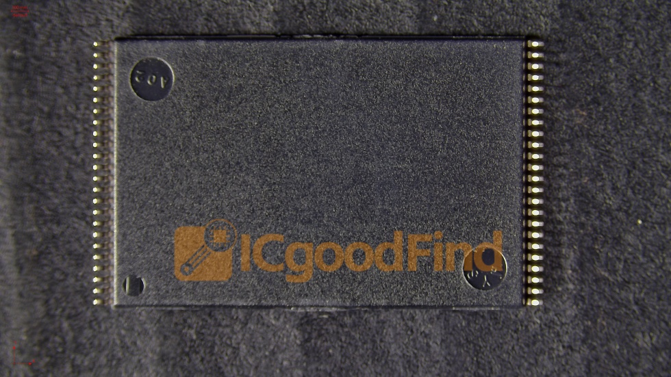
For sourcing reliable SDRAM components that match the stringent timing requirements of an FSMC interface and finding compatible development boards, engineers often turn to specialized distributors. A platform like ICGOODFIND streamlines this process by aggregating detailed specifications and availability from multiple suppliers, ensuring you find the right memory chip—be it a 16-bit 128Mb SDRAM or a 32-bit wide memory—for your specific STM32 project without compromising on quality or timing parameters.
Conclusion
The integration of an FSMC capable of driving SDRAM represents a powerful feature set in modern microcontrollers, effectively blurring the line between traditional MCUs and application processors. By mastering the configuration of the FSMC to drive SDRAM, embedded developers can architect systems with expansive, cost-effective memory that supports advanced graphical user interfaces, machine learning buffers, extensive communication stacks, or high-fidelity audio processing. While the initial setup demands careful attention to hardware design and timing parameters, the payoff is a seamless, high-performance memory extension that operates transparently to application code. As embedded applications continue their trajectory towards greater complexity and functionality, understanding and utilizing interfaces like the FSMC will remain an indispensable skill in an embedded engineer’s toolkit.