


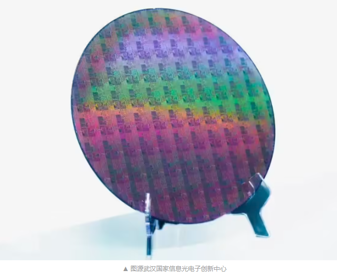
On September 28, the Wuhan National Information Optoelectronics Innovation Center announced the release of China’s first fully domestic 12-inch silicon photonics process design kit (PDK/ADK/TDK), marking the achievement of full-process standardization from design and manufacturing to testing and packaging.
Silicon photonics technology integrates microelectronics and photonics, enabling higher data transmission rates and lower power consumption. It serves as a foundational technology for 5G/6G and AI computing networks, while also bypassing reliance on EUV lithography systems. This unified toolkit streamlines collaboration across the supply chain, significantly shortening development cycles and reducing manufacturing costs. The kit already meets mass production requirements and is supporting leading companies in trial production of high-speed silicon photonics chips.
The breakthrough has attracted strong industry interest, with over 40 enterprises, universities, and institutions engaging in collaborations—more than ten of which have entered substantive cooperation phases. Under the "World Optic Valley" initiative, Wuhan aims to establish a 12-inch silicon-based photoelectronic integrated process line by 2030, targeting a position among the global top three in specialized silicon photonics manufacturing.
ICgoodFind : This kit resolves key bottlenecks in silicon photonics mass production, accelerating China’s path toward self-reliance in photonic chip technology.


